

Written by students who passed Immediately available after payment Read online or as PDF Wrong document? Swap it for free 4.6 TrustPilot
logo-home
Document preview thumbnail
Preview 2 out of 15 pages
Exam (elaborations)

Chapter 6 CCD/CMOS Exam Questions Correctly Answered.

Document preview thumbnail
Preview 2 out of 15 pages

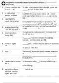
Chapter 6 CCD/CMOS Exam Questions Correctly Answered. 1. charge-coupled de- The oldest indirect conversion digital radiography systems used vices (CCDS) to acquire the digital image. 2. scintillation/ lenses or fiber 3. size/ light to electrical charge 4. analog-to-digital con- verter (ADC) 5. photosensitive recep- tor In a CCD system, x-ray photons interact with a material and the signal is transmitted by or optics to the CCD. During the transmission process, the lenses reduce the of the projected visible light image and transfer the image to one or more small capacitors that convert to . This charge is stored in a sequential pattern and released line by line and sent to an . A and electronics embedded into a substrate material in a silicon chip make up a CCD. 6. Incident light from a scintillator strikes the detector and electron/hole pairs are produced in the silicon. 7. light The number of electron/hole pairs is related to the amount of that is absorbed. 8. electrostatic forces The electrons are held by in the array until the charge is read out to from the image. 9. polysilicon layer, sili- con dioxide layer, sili- con substrate The chip is made up of a layer, layer, and a . 10. polysilicon The layer is coated with a photosensitive material and contains electronic gates. 11. silicon dioxide/ silicon substrate The layer is an insulator and the contains the charge storage area. 12. detector element (del) Each pixel or contains three electrodes that hold the electrons in a electrical potential wall. 13. voltage gates/ elec- trons 14. readout row/ "bucket brigade scheme" The dels are formed by that, at readout, are opened and closed like gates to allow the flow of . To collect the charge on the silicon chips, the voltage sign is changed on the electrodes within each del, moving the electrons by rows down the columns until the is reached. This is known as what? 15. amplifier Once the readout row is reached, the data are sent sequentially to the sense and are then digitized. 16. electrons There can be issues with overfill in the dels, which causes excessive to spill out of the del into an adjacent del. 17. "blooming" This is handled by building overflow drains into the array to reduce or prevent this " " ettect. 18. 5 cm x 5 cm Because of high cost of a CCD chip, it is not practical to manufacture CCD chips any larger than . 19. 2 to 4 cm Most chips range from to . 20. CCD The image has to be matched to the size of the , which implies that the image must be reduced in size. 21. scintillator, light collec- tion components, and noise 22. scintillator Reducing the image size involves several factors that contribute to the quality of the image including , , and . The type of and the way it is constr

Content preview

Chapter 6 CCD/CMOS Exam Questions Correctly
Answered.
1. charge-coupled de- The oldest indirect conversion digital radiography systems used
vices (CCDS) to acquire the digital image.

2. scintillation/ In a CCD system, x-ray photons interact with a material
lenses or fiber and the signal is transmitted by or optics to the
CCD.
3. size/ light to
electrical charge During the transmission process, the lenses reduce the
of the projected visible light image
and transfer the image to one or more small capacitors that
4. analog-to-digital
convert to .
con- verter (ADC)
This charge is stored in a sequential pattern and released line by
5. photosensitive
line and sent to an .
recep- tor
A and electronics embedded into a substrate
material in a silicon chip make up a CCD.

6. Incident light from a scintillator strikes the detector and electron/hole
pairs
are produced in the silicon.

7. light The number of electron/hole pairs is related to the amount
of

that is absorbed.

8. electrostatic forces The electrons are held by in the array until the charge is
read out
to from the image.

9. polysilicon layer, substrate
sili- con dioxide
layer, sili- con
1/
15

, Chapter 6 CCD/CMOS Exam Questions Correctly
Answered.
The chip is made up of a layer, layer, and a .

10. polysilicon The layer is coated with a photosensitive material and
contains
electronic gates.

11. silicon dioxide/ The layer is an insulator and the contains
silicon substrate the charge storage area.


2/
15

Document information

Uploaded on
July 16, 2025
Number of pages
15
Written in
2024/2025
Type
Exam (elaborations)
Contains
Questions & answers
$15.49

Wrong document? Swap it for free Within 14 days of purchase and before downloading, you can choose a different document. You can simply spend the amount again.
Written by students who passed
Immediately available after payment
Read online or as PDF

Seller avatar
Reputation scores are based on the amount of documents a seller has sold for a fee and the reviews they have received for those documents. There are three levels: Bronze, Silver and Gold. The better the reputation, the more your can rely on the quality of the sellers work.
Nursewendo
3.7
(22)
Sold
71
Followers
19
Items
4976
Last sold
2 months ago


Why students choose Stuvia

Created by fellow students, verified by reviews

Quality you can trust: written by students who passed their tests and reviewed by others who've used these notes.

Didn't get what you expected? Choose another document

No worries! You can instantly pick a different document that better fits what you're looking for.

Pay as you like, start learning right away

No subscription, no commitments. Pay the way you're used to via credit card and download your PDF document instantly.

Student with book image

“Bought, downloaded, and aced it. It really can be that simple.”

Alisha Student

Working on your references?

Create accurate citations in APA, MLA and Harvard with our free citation generator.

Working on your references?

Frequently asked questions

