ECE3201 Spring 2026
Homework #1 Solution
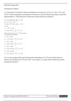
3.1 Find values of the intrinsic carrier concentration ni for silicon at −55°C, 0°C, 20°C, 75°C, and
125°C. At each temperature, what fraction of the atoms is ionized? Recall that a silicon crystal has
approximately 5 × 10²² atoms/cm3. What did you learn through this question?
3.6 In a boron-doped silicon layer with impurity concentration of 1017/cm3, find the hole and
electron concentrations at 27°C and 125°C. Is the result n- or p-type silicon? What did you learn
through this question?
Explore our developer-friendly HTML to PDF API Printed using PDFCrowd HTML to PDF
,3.7 Find the end-to-end resistance of a bar 15-µm long, 3-µm wide, and 1-µm thick, made of the
following materials at 25°C:
(a)intrinsic silicon
(b)n-doped silicon with ND = 5 × 10¹⁶/cm3
(c)n-doped silicon with ND = 5 × 10¹⁸/cm3
(d)p-doped silicon with NA = 5 × 10¹⁶/cm3
(e)aluminum with resistivity of 2.8 µΩ·cm
For intrinsic silicon, use the data in Table 3.1. For doped silicon, assume μn = 3μp = 1200 cm2/V ·
s. (Recall that R = ρL/A.)
For intrinsic silicon, use the data in Table 3.1 in the Summary Tables supplement found online at
www.oup. com/he/sedra-smith8e
Explore our developer-friendly HTML to PDF API Printed using PDFCrowd HTML to PDF
,3.14 If, for a particular junction, the acceptor concentration is 1017/cm3 and the donor
concentration is 1016/cm3, find the junction built-in voltage. Assume ni = 1.5 × 10¹⁰/cm3. Also, find
the width of the depletion region (W) and its extent in each of the p and n regions when the junction
terminals are left open. Calculate the magnitude of the charge stored on either side of the junction.
Assume that the junction area is 10 µm2. What did you learn through this question?
Explore our developer-friendly HTML to PDF API Printed using PDFCrowd HTML to PDF
, Explore our developer-friendly HTML to PDF API Printed using PDFCrowd HTML to PDF
Homework #1 Solution
3.1 Find values of the intrinsic carrier concentration ni for silicon at −55°C, 0°C, 20°C, 75°C, and
125°C. At each temperature, what fraction of the atoms is ionized? Recall that a silicon crystal has
approximately 5 × 10²² atoms/cm3. What did you learn through this question?
3.6 In a boron-doped silicon layer with impurity concentration of 1017/cm3, find the hole and
electron concentrations at 27°C and 125°C. Is the result n- or p-type silicon? What did you learn
through this question?
Explore our developer-friendly HTML to PDF API Printed using PDFCrowd HTML to PDF
,3.7 Find the end-to-end resistance of a bar 15-µm long, 3-µm wide, and 1-µm thick, made of the
following materials at 25°C:
(a)intrinsic silicon
(b)n-doped silicon with ND = 5 × 10¹⁶/cm3
(c)n-doped silicon with ND = 5 × 10¹⁸/cm3
(d)p-doped silicon with NA = 5 × 10¹⁶/cm3
(e)aluminum with resistivity of 2.8 µΩ·cm
For intrinsic silicon, use the data in Table 3.1. For doped silicon, assume μn = 3μp = 1200 cm2/V ·
s. (Recall that R = ρL/A.)
For intrinsic silicon, use the data in Table 3.1 in the Summary Tables supplement found online at
www.oup. com/he/sedra-smith8e
Explore our developer-friendly HTML to PDF API Printed using PDFCrowd HTML to PDF
,3.14 If, for a particular junction, the acceptor concentration is 1017/cm3 and the donor
concentration is 1016/cm3, find the junction built-in voltage. Assume ni = 1.5 × 10¹⁰/cm3. Also, find
the width of the depletion region (W) and its extent in each of the p and n regions when the junction
terminals are left open. Calculate the magnitude of the charge stored on either side of the junction.
Assume that the junction area is 10 µm2. What did you learn through this question?
Explore our developer-friendly HTML to PDF API Printed using PDFCrowd HTML to PDF
, Explore our developer-friendly HTML to PDF API Printed using PDFCrowd HTML to PDF