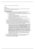
Name: ey .~ ECSE 321/422 Spring 2025
, Exam #2
Note: For Si, the bandgap is 1.12 eV, the intrinsic carrier concentration at 300K is 1.5 x 10'%/cm3,
and the relative permittivity is 11.8. The permittivity of free space is 8.85 x 10 14 F/em. 1 pm=
1x104cm.
Each problem is worth 10 points
1. Given a piece of Si at room temperature that is initially uniformly illuminated with light such that
electron-hole pairs are generated at a rate of 10'°/cm®*s throughout the entire sample. The mean
lifetime for electrons and holes is 10ps. The Si is doped with phosphorus at a concentration of
10'%/cm3. The diffusion coefficients for electrons and holes in this material are 36 cm*/s and 12 cm?/s,
respectively. The light source is then shut off.
a. Calculate the separation in the quasi Fermi levels for this sample Sus after turning off the
light source. (8 points)
b. Calculate the separation between the quasi Fermi level for the minority carriers and the
equilibrium quasi Fermi level Sus after turning off the light source. (2 points)
2. Consider a long, thin rectangular Si rod at room temperature that is uniformly doped with phosphorus
at a concentration of 10'¢/cm>. The electron and hole lifetimes are both 10us. The mobilities for
electrons and holes are 1390 cm?/V*s and 463 cm?/V*s, respectively. The rod is uniformly
illuminated with light on its left face such that electron-hole pairs are generated at a rate of 10'%/cm**
in a very thin region at the left end of the rod.
a. Calculate the minority carrier concentration at a distance of 0.005 cm from the region of
illumination. (8 points)
b. Calculate the current density associated with the minority carriers at a distance of 0.005 cm
from the region of illumination. (2 points)
3. Consider an ideal p-n junction with a cross-sectional area of 0.001 cm? under equilibrium conditions
at room temperature. The minority carrier concentrations in the neutral regions of this structure are
2250 /cm? and 4.5 x 10*/cm?. The mobility of electrons in the n-type region is higher than the
mobility of electrons in the p-type region. For this junction, calculate the penetration depth of the
transition region into the more heavily doped side of this p-n junction.
4. Consider a direct bandgap semiconductor that was illuminated by photons. You observe that this
semiconductor emits light long after the illumination has stopped. Using a simplified energy band
diagram and some descriptive text, provide an explanation of your observations.
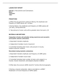
,5. The following plot presents electron and hole concentrations in a piece of silicon as a function of time.
Using concepts covered in class, do the following:
a. Based on the specific information given in the plot, what two things can you say about this
particular piece of silicon when it is under equilibrium conditions? (2 points)
Describe what was happening to the piece of silicon for t <0s. (4 points)
Provide a brief description of what happened in the piece of silicon for t > 0s. (4 points)
I > I > | ¥ I Y
Ap +p,=11x10%cm >
pw0
10 F ’/ :
| /]
py =10 15¢m 3
Carrier concentration (cm ~3)
An=10"%cm 3
—_
S
—_
o
dn=Ane-t/7
Indn=InAn—t/v
(F%]
—
[e]
—
1012 L
0 10 20 30 40 50
t (ns)
6. Consider an ideal p-n junction under equilibrium conditions where the built-in electric field penetrates
deeper into the n-type side of the metallurgical junction than the p-type side:
a. Sketch a cross-sectional diagram of this p-n junction showing all relevant regions. Indicate
the location and direction of the electric field. (4 points)
Make a sketch of the simplified energy band diagram for this p-n junction (no calculations
are necessary. Relative energy positions are sufficient). (4 points)
List two important assumptions about ideal p-n junctions. (2 points)
, /ot &
, Exam #2
Note: For Si, the bandgap is 1.12 eV, the intrinsic carrier concentration at 300K is 1.5 x 10'%/cm3,
and the relative permittivity is 11.8. The permittivity of free space is 8.85 x 10 14 F/em. 1 pm=
1x104cm.
Each problem is worth 10 points
1. Given a piece of Si at room temperature that is initially uniformly illuminated with light such that
electron-hole pairs are generated at a rate of 10'°/cm®*s throughout the entire sample. The mean
lifetime for electrons and holes is 10ps. The Si is doped with phosphorus at a concentration of
10'%/cm3. The diffusion coefficients for electrons and holes in this material are 36 cm*/s and 12 cm?/s,
respectively. The light source is then shut off.
a. Calculate the separation in the quasi Fermi levels for this sample Sus after turning off the
light source. (8 points)
b. Calculate the separation between the quasi Fermi level for the minority carriers and the
equilibrium quasi Fermi level Sus after turning off the light source. (2 points)
2. Consider a long, thin rectangular Si rod at room temperature that is uniformly doped with phosphorus
at a concentration of 10'¢/cm>. The electron and hole lifetimes are both 10us. The mobilities for
electrons and holes are 1390 cm?/V*s and 463 cm?/V*s, respectively. The rod is uniformly
illuminated with light on its left face such that electron-hole pairs are generated at a rate of 10'%/cm**
in a very thin region at the left end of the rod.
a. Calculate the minority carrier concentration at a distance of 0.005 cm from the region of
illumination. (8 points)
b. Calculate the current density associated with the minority carriers at a distance of 0.005 cm
from the region of illumination. (2 points)
3. Consider an ideal p-n junction with a cross-sectional area of 0.001 cm? under equilibrium conditions
at room temperature. The minority carrier concentrations in the neutral regions of this structure are
2250 /cm? and 4.5 x 10*/cm?. The mobility of electrons in the n-type region is higher than the
mobility of electrons in the p-type region. For this junction, calculate the penetration depth of the
transition region into the more heavily doped side of this p-n junction.
4. Consider a direct bandgap semiconductor that was illuminated by photons. You observe that this
semiconductor emits light long after the illumination has stopped. Using a simplified energy band
diagram and some descriptive text, provide an explanation of your observations.
,5. The following plot presents electron and hole concentrations in a piece of silicon as a function of time.
Using concepts covered in class, do the following:
a. Based on the specific information given in the plot, what two things can you say about this
particular piece of silicon when it is under equilibrium conditions? (2 points)
Describe what was happening to the piece of silicon for t <0s. (4 points)
Provide a brief description of what happened in the piece of silicon for t > 0s. (4 points)
I > I > | ¥ I Y
Ap +p,=11x10%cm >
pw0
10 F ’/ :
| /]
py =10 15¢m 3
Carrier concentration (cm ~3)
An=10"%cm 3
—_
S
—_
o
dn=Ane-t/7
Indn=InAn—t/v
(F%]
—
[e]
—
1012 L
0 10 20 30 40 50
t (ns)
6. Consider an ideal p-n junction under equilibrium conditions where the built-in electric field penetrates
deeper into the n-type side of the metallurgical junction than the p-type side:
a. Sketch a cross-sectional diagram of this p-n junction showing all relevant regions. Indicate
the location and direction of the electric field. (4 points)
Make a sketch of the simplified energy band diagram for this p-n junction (no calculations
are necessary. Relative energy positions are sufficient). (4 points)
List two important assumptions about ideal p-n junctions. (2 points)
, /ot &