

2003 IEEE International Interconnect Technology Conference (IITC), pp. 74-76, San Francisco Airport, CA, June 2 - 4, 2003.
Evaluation Procedures for Wafer Bonding and Thinning of
Interconnect Test Structures for 3D ICs
J.-Q. Lu, A. Jindal, Y. Kwon, J.J. McMahon, M. Rasco*, R. Augur*, T.S. Cale, and R.J. Gutmann
Focus Center – New York, Rensselaer Polytechnic Institute, Troy, NY 12180;
*International Sematech, 2706 Montopolis Drive, Austin TX 78741
Abstract -- Electrical and mechanical impacts of wafer of our approach, where fully processed wafers (with
bonding and thinning processes required for three- multilevel on-chip interconnects) are aligned and bonded
dimensional (3D) IC fabrication have been evaluated with with a dielectric glue, followed by top-wafer thinning and
interconnect structures. In addition to the bonding and inter-wafer interconnection. Among other process steps,
thinning required for a two-level 3D IC stack, an additional wafer bonding and thinning involve thermal and mechanical
bonding and thinning process is used along with dielectric processes; their impacts on the processed wafers need to be
glue ashing to expose the previously tested interconnect evaluated to qualify the process.
structures. This procedure permits evaluation of bonding Various procedures are developed for specific
and thinning integrity without inter-wafer interconnect evaluation purposes. Three evaluation procedures are
processing. Promising results on wafers with oxide inter- discussed in this paper: (1) visual inspection using thermal-
level dielectric (ILD) have been obtained, while some coefficient-of-expansion (TCE) matched glass wafers, (2)
damages observed with the porous low-k ILD. mechanical bonding strength tests using four-point (4-pt)
bending/delamination technique, and (3) electrical tests of
I. Introduction the processed wafers using a procedure that involves
additional bonding, thinning and dielectric glue ashing.
One of the emerging architectures/technologies for In order to visually evaluate the bonding and thinning
future chips is wafer-level three-dimensional (3D) integrity, an interconnect test structure wafer with 900 nm
integration [1,2], i.e., fabrication of functional components topological features across the Al test pads was bonded onto
(e.g., logic and memory) on separate wafers, followed by a TCE-matched glass wafer using benzocyclobutene (BCB).
wafer aligning, bonding, thinning and vertical inter-wafer The use of TCE matched glass allows visual inspection of
interconnection [3]. The 3D integration offers high the bonding and thinning integrity through the glass wafer.
interconnect performance by reducing delays of global The Si substrate was then completely removed by a three-
interconnects [2] and high functionality with heterogeneous step thinning process: grinding, polishing and tetramethyl-
integration of materials, devices, and signals [1-4]. Initial ammonium hydroxide (TMAH) wet etching. Typically the
focus of the 3D integration has been on microprocessors, grinding and polishing processes thin the Si substrate to 30 –
application specific ICs (ASICs), and memories, but 50 µm. Subsequent wet etching stops at the oxide layer,
extensions to RF, analog, optical, and micro-electro- leaving a transparent Cu/oxide interconnect structures on the
mechanical systems (MEMS) are also being pursued [1-5]. glass wafer. Fig. 2 shows an image of transparent Cu/oxide
One of the fundamental issues in all 3D IC interconnect structures on a TCE-matched glass wafer.
implementations [2-11] is the 3D processing compatibility Detailed optical microscopy inspection indicates a defect-
with advanced semiconductor processing protocols. We free bonding interface with damage-free interconnect
have developed procedures to evaluate the impact of wafer patterns maintained. For similarly processed wafers with
bonding and thinning processes on the performance and Bridge Via Plug Via
yield of wafers without requiring inter-wafer interconnect Dielectric
processing. Wafers with state-of-the-art two-level back-end 3rd Level Substrate
Device
copper interconnect test structures with two types of inter- (Thinned surface
Substrate)
level dielectrics (ILDs) are evaluated. Promising results are
obtained on wafers with oxide ILD, while wafers with Bond
Dielectric (Face-to-back)
porous low-k ILD show some damage. Both the types of 2nd Level Substrate
Device
wafers were provided by International SEMATECH. (Thinned surface
Substrate)
II. Experimental Results and Discussion Bond
(Face-to-face)
The experimental procedures to evaluate the wafer 1st Level Multi-level on-chip interconnects
Device
bonding and thinning processes are based on our 3D Substrate
surface
integration approach, which is also referred to as monolithic
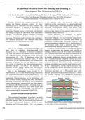
Fig. 1. Schematic of a monolithic 3D IC test vehicle using wafer bonding,
high density multifunctional integration (HDMI) or hyper- showing bonding interface, vertical inter-chip vias (plug- and bridge-type),
integration (see [3] for more details). Fig. 1 is a schematic and "face-to-face" and "face-to-back" bonding.
74 0-7803-7797-4/03/$17.00 ©2003 IEEE
Evaluation Procedures for Wafer Bonding and Thinning of
Interconnect Test Structures for 3D ICs
J.-Q. Lu, A. Jindal, Y. Kwon, J.J. McMahon, M. Rasco*, R. Augur*, T.S. Cale, and R.J. Gutmann
Focus Center – New York, Rensselaer Polytechnic Institute, Troy, NY 12180;
*International Sematech, 2706 Montopolis Drive, Austin TX 78741
Abstract -- Electrical and mechanical impacts of wafer of our approach, where fully processed wafers (with
bonding and thinning processes required for three- multilevel on-chip interconnects) are aligned and bonded
dimensional (3D) IC fabrication have been evaluated with with a dielectric glue, followed by top-wafer thinning and
interconnect structures. In addition to the bonding and inter-wafer interconnection. Among other process steps,
thinning required for a two-level 3D IC stack, an additional wafer bonding and thinning involve thermal and mechanical
bonding and thinning process is used along with dielectric processes; their impacts on the processed wafers need to be
glue ashing to expose the previously tested interconnect evaluated to qualify the process.
structures. This procedure permits evaluation of bonding Various procedures are developed for specific
and thinning integrity without inter-wafer interconnect evaluation purposes. Three evaluation procedures are
processing. Promising results on wafers with oxide inter- discussed in this paper: (1) visual inspection using thermal-
level dielectric (ILD) have been obtained, while some coefficient-of-expansion (TCE) matched glass wafers, (2)
damages observed with the porous low-k ILD. mechanical bonding strength tests using four-point (4-pt)
bending/delamination technique, and (3) electrical tests of
I. Introduction the processed wafers using a procedure that involves
additional bonding, thinning and dielectric glue ashing.
One of the emerging architectures/technologies for In order to visually evaluate the bonding and thinning
future chips is wafer-level three-dimensional (3D) integrity, an interconnect test structure wafer with 900 nm
integration [1,2], i.e., fabrication of functional components topological features across the Al test pads was bonded onto
(e.g., logic and memory) on separate wafers, followed by a TCE-matched glass wafer using benzocyclobutene (BCB).
wafer aligning, bonding, thinning and vertical inter-wafer The use of TCE matched glass allows visual inspection of
interconnection [3]. The 3D integration offers high the bonding and thinning integrity through the glass wafer.
interconnect performance by reducing delays of global The Si substrate was then completely removed by a three-
interconnects [2] and high functionality with heterogeneous step thinning process: grinding, polishing and tetramethyl-
integration of materials, devices, and signals [1-4]. Initial ammonium hydroxide (TMAH) wet etching. Typically the
focus of the 3D integration has been on microprocessors, grinding and polishing processes thin the Si substrate to 30 –
application specific ICs (ASICs), and memories, but 50 µm. Subsequent wet etching stops at the oxide layer,
extensions to RF, analog, optical, and micro-electro- leaving a transparent Cu/oxide interconnect structures on the
mechanical systems (MEMS) are also being pursued [1-5]. glass wafer. Fig. 2 shows an image of transparent Cu/oxide
One of the fundamental issues in all 3D IC interconnect structures on a TCE-matched glass wafer.
implementations [2-11] is the 3D processing compatibility Detailed optical microscopy inspection indicates a defect-
with advanced semiconductor processing protocols. We free bonding interface with damage-free interconnect
have developed procedures to evaluate the impact of wafer patterns maintained. For similarly processed wafers with
bonding and thinning processes on the performance and Bridge Via Plug Via
yield of wafers without requiring inter-wafer interconnect Dielectric
processing. Wafers with state-of-the-art two-level back-end 3rd Level Substrate
Device
copper interconnect test structures with two types of inter- (Thinned surface
Substrate)
level dielectrics (ILDs) are evaluated. Promising results are
obtained on wafers with oxide ILD, while wafers with Bond
Dielectric (Face-to-back)
porous low-k ILD show some damage. Both the types of 2nd Level Substrate
Device
wafers were provided by International SEMATECH. (Thinned surface
Substrate)
II. Experimental Results and Discussion Bond
(Face-to-face)
The experimental procedures to evaluate the wafer 1st Level Multi-level on-chip interconnects
Device
bonding and thinning processes are based on our 3D Substrate
surface
integration approach, which is also referred to as monolithic
Fig. 1. Schematic of a monolithic 3D IC test vehicle using wafer bonding,
high density multifunctional integration (HDMI) or hyper- showing bonding interface, vertical inter-chip vias (plug- and bridge-type),
integration (see [3] for more details). Fig. 1 is a schematic and "face-to-face" and "face-to-back" bonding.
74 0-7803-7797-4/03/$17.00 ©2003 IEEE


