UNIT 1
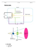
MOSFET
MOSFET stands for metal oxide semiconductor field effect transistor. It is capable of
voltage gain and signal power gain. The MOSFET is the core of integrated circuit designed as
thousands of these can be fabricated in a single chip because of its very small size. It is a four
terminals device. The drain and source terminals are connected to the heavily doped regions.
The gate terminal is connected top on the oxide layer and the substrate or body terminal is
connected to the intrinsic semiconductor.
These devices can be classified into two types viz., depletion-type and enhancement-
type, depending on whether they possess a channel in their default state or no, respectively.
Further, each of them can be either p-channel or n-channel devices as they can have their
conduction current due to holes or electrons respectively.
Fig 1 MOSFET
• Operation with Zero Gate Voltage
Two back-to-back diodes, High Resistance (Giga Ohms), No Current Flow
,• Creating a Channel for Current Flow
Application of gate source voltage will create a channel for current flow.
• Applying a small VDS
Application of VDS will start a current flow between the drain and source terminals.
• Operation as VDS is increased
As Vds increases the following changes will happen
,