Electronic Circuit
Design &
Manufacture
Unit 34
Fahim Mohammed
RM
, Unit 34 PCB Design and Manufacturing Techniques Assignment 1
In this new unit, I will begin by describing the processes used in the design of both a single &
multi-layer PCB for electronic circuits of different complexity. Firstly, PCB stands for
‘Printed Circuit Board’, but it can also be called ‘Printed Wiring Boards (or Cards)’. Now, a
PCB mechanically aids & electrically bonds other components using their tracks & other
features that are engraved from copper sheets laminated onto a substrate that isn’t conductive;
the conductive metal parts that transfer energy are usually created from copper. There is
another layer known as silkscreen that is on top of the board & this shows what goes where.
Below is a diagram of a single layer PCB
The diagram below shows a double layer PCB, which has 2 layers of copper foil instead of
one.
Furthermore, if the complexity increases this means that more than 2 layers are need
in the PCB, so other layers of copper can be added to the ones shown in the diagram
above.
Below shows a multi-layer PCB with more than 1 copper foil layer.
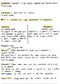
To design a PCB, a PCB designer is required & what this person would do is make a
schematic before actually designing the board; the schematic will contain a series of symbols
that represent aspects of the circuit, such as resistors, nodes, switches, diodes & may more.
Once the circuit design is taken in a schematic, it’s then translated into an electronic design
automation (EDA) software package & the design is exported into an industry standard
format.
After the designer has a CAD file, the PCB can be manufactured; the dimensions of the PCB,
along with the amount of layers there’ll be are decided & all the components are positioned &
laid out accurately. Additionally, there are a variety of requirements for diverse boards, so
the designer will be able to come to a conclusion whether a n SMT is needed.
Lastly, the PCB will go through a special testing known as ‘white box’, & this’ll correctly be
fabricated & ensure its structured well. The objective is to test for every possible output to
make sure the PCB is working just how the designer wanted it to. There is another testing
method, known as ‘black box’ that only tests inputs & outputs.
P1 Fahim Mohammed
Design &
Manufacture
Unit 34
Fahim Mohammed
RM
, Unit 34 PCB Design and Manufacturing Techniques Assignment 1
In this new unit, I will begin by describing the processes used in the design of both a single &
multi-layer PCB for electronic circuits of different complexity. Firstly, PCB stands for
‘Printed Circuit Board’, but it can also be called ‘Printed Wiring Boards (or Cards)’. Now, a
PCB mechanically aids & electrically bonds other components using their tracks & other
features that are engraved from copper sheets laminated onto a substrate that isn’t conductive;
the conductive metal parts that transfer energy are usually created from copper. There is
another layer known as silkscreen that is on top of the board & this shows what goes where.
Below is a diagram of a single layer PCB
The diagram below shows a double layer PCB, which has 2 layers of copper foil instead of
one.
Furthermore, if the complexity increases this means that more than 2 layers are need
in the PCB, so other layers of copper can be added to the ones shown in the diagram
above.
Below shows a multi-layer PCB with more than 1 copper foil layer.
To design a PCB, a PCB designer is required & what this person would do is make a
schematic before actually designing the board; the schematic will contain a series of symbols
that represent aspects of the circuit, such as resistors, nodes, switches, diodes & may more.
Once the circuit design is taken in a schematic, it’s then translated into an electronic design
automation (EDA) software package & the design is exported into an industry standard
format.
After the designer has a CAD file, the PCB can be manufactured; the dimensions of the PCB,
along with the amount of layers there’ll be are decided & all the components are positioned &
laid out accurately. Additionally, there are a variety of requirements for diverse boards, so
the designer will be able to come to a conclusion whether a n SMT is needed.
Lastly, the PCB will go through a special testing known as ‘white box’, & this’ll correctly be
fabricated & ensure its structured well. The objective is to test for every possible output to
make sure the PCB is working just how the designer wanted it to. There is another testing
method, known as ‘black box’ that only tests inputs & outputs.
P1 Fahim Mohammed