Gate Implementation
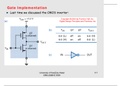
Last time we discussed the CMOS inverter:
University of KwaZulu-Natal 1
4-1
ENEL2EBH2 2009
, CMOS Logic
We noted that a MOS transistor is a voltage controlled device:
The voltage applied to the gate terminal controls the
resistance between the drain and source terminals.
In logic applications the MOS device is either switched OFF
(very high drain to source resistance, in excess of 106 ohms)
or ON (very low drain to source resistance, less than 10 ohms).
Thus the MOS device can be modeled as a switch.
NMOS (ON for gate at logic 1) and PMOS (ON for gate at logic
0).
Using NMOS and PMOS as complement devices gives CMOS.
University of KwaZulu-Natal 2
4-2
ENEL2EBH2 2009