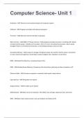
Computer Science
Computer Science Paper 1 Control Unit - ANS-A register in the cpu that controls and coordinates the activities of the cpu directing the flow of data Bus - ANS-a series of connectors that transfer signals between internal components Memory Read - ANS-causes data from the addressed location in RAM to be placed on the data bus Memory Write - ANS-Causes data on the data bus to be written into the addressed location. Bus Request - ANS-Indicates that a device is requesting the use of the data bus Bus Grant - ANS-Indicates that the CPU has granted access to the data bus. System bus - ANS-collective term for address, data and control bus Data bus - ANS-A bi-directional path for moving data and instructions between system components Clock - ANS-used to synchronize operations Control bus - ANS-A bi-directional bus to transmit command, timing and specific status information between system components Address bus - ANS-A one directional bus that transmits memory addresses that are used as operands in programming instructions, so that data can be retrieved from main memory ALU - ANS-Arithmetic-Logic unit, preforms logical and arithmetic operations on data e.g. ADD, SUBTRACT, shift operations or Boolean logic Registers - ANS-High speed memory cells, all arithmetic and logic happens in these, typically there are 16 general purpose registers in a CPU, they are very fast Accumulator - ANS-A special purpose register which stores the result of calculations made by the ALU Program Counter (PC) - ANS-Holds the address of the next instruction to be executed, this can be the next instruction in a sequence of instructions, or a branch/ jump Current instruction register (CIR) - ANS-stores the actual instruction that is being decoded Memory address register (MAR) - ANS-stores the address of instructions and data that need to be fetched from or sent to memory Memory data register (MDR) - ANS-stores the data which is to be sent or fetched from memory Interrupt registers - ANS-generates and detects interrupts Fetch Decode Execute register sequence - ANS-PC MAR Address Bus Memory Data bus MDR CIR Decode Unit MAR Address Bus Main Memory Fetch phase - ANS-- Instructions pulled from memory and stored in main memory. - Program Counter (a register) stores the address location of the instruction - Program Counter and instructions are placed in the Instruction Register (IR) - Program Counter is incremented by 1 Decode phase - ANS-1. Instruction in CIR is decoded 2. Instruction is split into opcode and operand 3. the operand determines the type of instruction - if its the address of the data used with the operation it is copied into the MAR - if it the actual data to be operated on it is copied into the MDR 4. the data to be operated on is passed into the ALU/ acc Execute phase - ANS-The appropriate instruction/ opcode is carried out on the data/ operand Main factors affecting preformance - ANS-- Clock speed - Number of cores - The amount and type of cache Clock speed - ANS-The system clock generates a series of signals (1 or 0) synchronising with the CPU operations. The CPU cannot preform faster than the system clock. Positives of increasing clock speed - ANS-You can carry out more instructions in a given time; improved performance What is clock speed measured in? - ANS-Hz Negatives of increasing clock speed - ANS-more heat generated meaning computers must be cooled (either with heat sync/fan or water/oil cooling) Positive of multiple cores - ANS-may speed processing as concurrency is available negatives of multiple cores - ANS-complicated circuitry (more expensive) doesn't always improve performance Positives of increasing cache size - ANS-less time fetching data; improved performance Negatives of increasing cache size - ANS-expensive, physically further from cpu and thus slower Level 1 cache - ANS-Small but extremely fast Level 2 cache - ANS-fairly fast and medium sized Level 3 cache - ANS-slower and bigger Pipelining - ANS-When the computer architecture allows the next instruction to be fetched at the same time as the processor is preforming arithmetic or logical operations. (buffer close to the processor) Bottleneck Address bus - ANS-The width of the address bus determines the maximum possible capacity of the system e.g. is the address bus was 8 lines, the maximum it could transmit would be 256 Bottleneck Data bus - ANS-A wider bus can transmit larger values/ more bits per instruction Von Neumann architecture - ANS-Instructions and data: - Share memory - Share bus system - Stored in same format - Same bit size for memory - Single CPU and ALU Harvard architecture - ANS-Instructions and data are:
Written for
- Institution
- Graduation in computer science
- Module
- Graduation in computer science
Document information
- Uploaded on
- July 23, 2024
- Number of pages
- 69
- Written in
- 2023/2024
- Type
- Exam (elaborations)
- Contains
- Questions & answers
