(01) Computer Systems
1.1.1 Structure and function of the processor
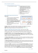
(a)The Arithmetic Logic Unit and Control Unit
Control Unit ‐
Controls and monitors attached hardware,
ensures commands are executed
Controls the input and output of data ‐
signals are forwarded to the right place at the
right time. Controls flow of data in FDE Cycle
It decodes instructions into multiple steps to
simultaneously execute
It Executes Instructions and stores results
back in memory
The ALU is divided in 2 parts; Output stored in accumulator to be collected by the data bus.
Arithmetic ‐ performs calculations on integers and floating point numbers
Logic ‐ deals with logic and comparisons, can also perform shifts (1.4.1(i) – Shifts)
Registers (PC, MAR, MDR, CIR) (Accumulator Overleaf) ‐ faster than Cache or RAM
A Register is a discrete memory location to hold temporary data. They are small pieces of fast
memory acting as a “Buffer”. There are general and special purpose registers all within the CPU.
The program counter’s value represents the address of the next instruction to be fetched and
executed. This address is given to the Memory address register when the cycle begins. The value
can only be altered by flow altering instructions such as Jump and Branch in LMC. The value it holds
might be in sequence or it might be executing a “jump”
The Memory address register stores the address of instructions and data to be fetched or written to
in the storage. It uses the address bus (locate) and data bus to read/write. This is then stored in the
MDR (for fetch), or results are taken from the MDR for write.
The Memory Data Register (Memory Buffer Register) holds a buffer of the data that has been read
or is to be written. If the data is an Instruction it is sent to the CIR, otherwise held until required for
processing. The MDR may also hold data waiting to be written.
If the data in the MDR is an instruction it is sent to the Current Instruction Register. Instructions are
represented as Opcode and Operand, the opcode is the instruction stored in the CIR for decoding,
the operand is either data (which is given to the MDR) or it is the address of the data (given to the
MAR to be fetched). The instruction will be decoded by the control unit, where it will be checked to
ensure it is a valid instruction. When the Program Counter increments a new FDE cycle begins
P a g e 2 | 81
Ravi Shah
1.1.1 Structure and function of the processor
(a)The Arithmetic Logic Unit and Control Unit
Control Unit ‐
Controls and monitors attached hardware,
ensures commands are executed
Controls the input and output of data ‐
signals are forwarded to the right place at the
right time. Controls flow of data in FDE Cycle
It decodes instructions into multiple steps to
simultaneously execute
It Executes Instructions and stores results
back in memory
The ALU is divided in 2 parts; Output stored in accumulator to be collected by the data bus.
Arithmetic ‐ performs calculations on integers and floating point numbers
Logic ‐ deals with logic and comparisons, can also perform shifts (1.4.1(i) – Shifts)
Registers (PC, MAR, MDR, CIR) (Accumulator Overleaf) ‐ faster than Cache or RAM
A Register is a discrete memory location to hold temporary data. They are small pieces of fast
memory acting as a “Buffer”. There are general and special purpose registers all within the CPU.
The program counter’s value represents the address of the next instruction to be fetched and
executed. This address is given to the Memory address register when the cycle begins. The value
can only be altered by flow altering instructions such as Jump and Branch in LMC. The value it holds
might be in sequence or it might be executing a “jump”
The Memory address register stores the address of instructions and data to be fetched or written to
in the storage. It uses the address bus (locate) and data bus to read/write. This is then stored in the
MDR (for fetch), or results are taken from the MDR for write.
The Memory Data Register (Memory Buffer Register) holds a buffer of the data that has been read
or is to be written. If the data is an Instruction it is sent to the CIR, otherwise held until required for
processing. The MDR may also hold data waiting to be written.
If the data in the MDR is an instruction it is sent to the Current Instruction Register. Instructions are
represented as Opcode and Operand, the opcode is the instruction stored in the CIR for decoding,
the operand is either data (which is given to the MDR) or it is the address of the data (given to the
MAR to be fetched). The instruction will be decoded by the control unit, where it will be checked to
ensure it is a valid instruction. When the Program Counter increments a new FDE cycle begins
P a g e 2 | 81
Ravi Shah