Samenvatting EM HC.5
You have two different types of electron microscopy
SEM information about the surface, focused beam on sample
TEM information on the inside, parallel beam on sample
SEM
With scan, you focus your electron beam on your sample,
convergent beam. This point is called a probe and you want it
as small as possible. The smaller your probe, the higher your
resolution and the better your imaging.
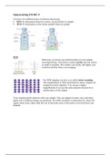
For SEM imaging you have a so called raster scanning.
The magnification is NOT performed by lenses. Signals are
assigned to pixels digitally. You can get a higher
magnification if you use the same amount of pixels for a
smaller piece of the sample.
Your scanning probe interacts with your sample. This can happen in many ways and many
depth, and so different things are produced. The SEM resolution is determines by where the
signal comes from, rather than the size of the probe (size of the probe is involved but is not
limited).
, Secondairy electrons (SE) electrons
from the sample emitted after being
knocked free by the probe.
Never accelerated by HT
Only have enough energy to escape
from near the surface
Carry most topographical information
Backscattered electrons (BSE)
electrons from the probe that scatter back.
Give material contrast (amount of
backscattering depends on Z)
More energetic that SE, still large
spread of energy losses
A lower kV of your electron
beam improves the resolution
because the depth of which
electrons are coming from
becomes better.
When you perform SEM you usually coat your sample with a conductive layer (sample
preperation). This is because not all probe electrons come out of your sample and you need to
allow them to go away (otherwise accumulation).
Prevents accumulation of electrons that lead to charging
Decrease surface work function () easier for SE to escape, more signal comes out
means better imaging
May obscure small features (a lot when coat is thicker than sample)
Interference with elemental analysis
Environmental SEM (ESEM) you avoid coating by reducing the vacuum which allows
charge dissipation. A drawback is that it effects signaling.
SEM detectors count electrons that come are derived from one point. So detectors have
NO pixels and generally don’t have single electron sensitivity. The more electrons derive
from a spot, the lighter that spot is. The orientation of your detector gives the “shadowing
effect” of SEM images.
You have two different types of electron microscopy
SEM information about the surface, focused beam on sample
TEM information on the inside, parallel beam on sample
SEM
With scan, you focus your electron beam on your sample,
convergent beam. This point is called a probe and you want it
as small as possible. The smaller your probe, the higher your
resolution and the better your imaging.
For SEM imaging you have a so called raster scanning.
The magnification is NOT performed by lenses. Signals are
assigned to pixels digitally. You can get a higher
magnification if you use the same amount of pixels for a
smaller piece of the sample.
Your scanning probe interacts with your sample. This can happen in many ways and many
depth, and so different things are produced. The SEM resolution is determines by where the
signal comes from, rather than the size of the probe (size of the probe is involved but is not
limited).
, Secondairy electrons (SE) electrons
from the sample emitted after being
knocked free by the probe.
Never accelerated by HT
Only have enough energy to escape
from near the surface
Carry most topographical information
Backscattered electrons (BSE)
electrons from the probe that scatter back.
Give material contrast (amount of
backscattering depends on Z)
More energetic that SE, still large
spread of energy losses
A lower kV of your electron
beam improves the resolution
because the depth of which
electrons are coming from
becomes better.
When you perform SEM you usually coat your sample with a conductive layer (sample
preperation). This is because not all probe electrons come out of your sample and you need to
allow them to go away (otherwise accumulation).
Prevents accumulation of electrons that lead to charging
Decrease surface work function () easier for SE to escape, more signal comes out
means better imaging
May obscure small features (a lot when coat is thicker than sample)
Interference with elemental analysis
Environmental SEM (ESEM) you avoid coating by reducing the vacuum which allows
charge dissipation. A drawback is that it effects signaling.
SEM detectors count electrons that come are derived from one point. So detectors have
NO pixels and generally don’t have single electron sensitivity. The more electrons derive
from a spot, the lighter that spot is. The orientation of your detector gives the “shadowing
effect” of SEM images.