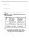
Real World Design
For more complex combinational problems with a larger number
of inputs, one can resort to the use of a minimization algorithm,
such as Quine-McCluskey.
In practice however most designs are implemented using
programmable Ics.
There are two basic categories of programmable logic circuits:
programmable logic devices (PLDs) which are used for medium
scale designs, and complex PLDs (CPLDs) or Field Programmable
Gate Arrays (FPGAs) for large scale designs.
It is recognized that design correctness is more important than
logic minimization, so device logic functionality is expressed
using high-level languages such as ABEL or VHDL.
Another design option for medium scale designs is to use a
medium scale integration (MSI) chip as the basis of the solution.
University of KwaZulu-Natal 1
8-1
ENEL2EBH2 2010
, Design Procedure
The design of a combinational circuit starts from the
specification of the problem and ends with a logic diagram or
netlist that describes a logic diagram. The steps followed are:
1. Specification: here, the specification of the needed circuit is
written down.
2. Formulation: here, Boolean equations or the truth table that
shows the relationship between the inputs and the outputs is
written down.
3. Optimization: here, two-level and multi-level optimization is
done. Draw a logic diagram or provide a netlist for the resulting
circuit using basic logic gates.
4. Technology Mapping: at this stage we transform the logic
diagram or netlist to anew diagram or netlist using the available
implementation technology.
5. Verification: at this stage you verify the correctness of the
design.
University of KwaZulu-Natal 2
8-2
ENEL2EBH2 2010