for
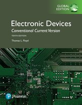
Electronic Devices
Tenth Edition
Global Edition
Thomas L. Floyd
ISBN-13: 978-1-29-222300-1
ISBN-10: 1-29-222300-6
, Contents
Solutions for End-of-Chapter Problems
Part 1: Problem Solutions......................................................................... 1
Chapter 1: Introduction to Semiconductors ................................................. 2
Chapter 2: Diodes and Applications .............................................................. 4
Chapter 3: Special-Purpose Diodes .............................................................. 19
Chapter 4: Bipolar Junction Transistors ..................................................... 28
Chapter 5: Transistor Bias Circuits ............................................................. 40
Chapter 6: BJT Amplifiers............................................................................ 58
Chapter 7: BJT Power Amplifiers................................................................ 76
Chapter 8: Field-Effect Transistors (FETs) ................................................ 87
Chapter 9: FET Amplifiers and Switching Circuits ................................. 104
Chapter 10: Amplifier Frequency Response ............................................... 114
Chapter 11: Thyristors .................................................................................. 128
Chapter 12: The Operational Amplifier ...................................................... 135
Chapter 13: Basic Op-Amp Circuits ............................................................ 149
Chapter 14: Special-Purpose Integrated Circuits....................................... 158
Chapter 15: Active Filters ............................................................................. 165
Chapter 16: Oscillators .................................................................................. 172
Chapter 17: Voltage Regulators ................................................................... 177
Part 2: Device Application Results ...................................................... 183
Part 3: Summary of Multisim and LT Spice Circuit Files by
Gary Snyder .............................................................................. 204
Part 4: Solutions Manual for Laboratory Exercises for
Electronic Devices..................................................................... 233
iii
Copyright © 2018 Pearson Education Ltd.
,Part 1
Problem Solutions
Chapter 1
Introduction to Semiconductors
Section 1-1 The Atom
1. Unlike in the Bohr model, the electrons in the quantum model do not exist in precise circular
orbits as particles. Three important principles underlie the quantum model: The wave-particle
duality principle, the uncertainty principle, and the superposition principle.
2. If a valence electron acquires sufficient amount of energy, called ionization energy, it can escape
from the outer shell and the atom’s influence. The escaped valence electron is called a free
electron.
3. 32.
4. The maximum number of electrons in shells 1 to 4 is 2, 8, 18, and 32, respectively, so the total
will be 60 electrons.
Section 1-2 Materials Used in Electronics
5. The materials represented in Figure 121 in the textbook are
(a) insulator (b) semiconductor (c) conductor
6. The valence electrons in germanium are in the fourth shell while those in silicon are in the third
shell, closer to the nucleus. This means that the germanium valence electrons are at higher energy
levels than those in silicon and, therefore, require a smaller amount of additional energy to escape
from the atom. This property makes germanium more unstable at high temperatures and results in
excessive reverse current.
7. 4.
Section 1-3 Current in Semiconductors
iv
, 8. The electron returns to the valence band of one of the silicon atoms in the crystal and fills an
existing hole. This is called recombination.
9. Current is produced in silicon at the conduction band and the valence band.
10. A valence electron can move into a nearby hole with little change in its energy level, thus leaving
another hole where it came from. Effectively, the hole has moved from one place to another in the
crystal structure. Thus, a hole current is effectively generated.
11. Since the valence electrons in the metal are free to move, the application of a voltage results in
current.
Section 1-4 N-Type and P-Type Semiconductors
12. When pentavalent atoms are introduced to the silicon crystal, they form covalent bonds with 4
silicon atoms. But one extra electron of the impurity atom is not part of any covalent bonds. It
becomes a free (conduction) electron, effectively increasing the number of majority carriers
(electrons in this case) in the crystal.
13. Antimony is a pentavalent (donor) material used for doping to increase free electrons. Boron is a
trivalent (acceptor) material used for doping to increase the holes.
Section 1-5 The PN Junction
14. As the pn junction forms, the free electrons from the n region diffuse through the junction into the
p region. This creates a thin layer of positive charge (donor ions) in the n region. When the
diffused electrons combine with holes in the p region, a thin layer of negative charges (acceptor
ions) is formed in the p region. Effectively, these two layers are depleted of any charge carriers.
15. The barrier potential of a diode represents an energy gradient that must be overcome by
conduction electrons and produces a voltage drop, not a source of energy.
Chapter 2
Diodes and Applications
Section 2-1 Diode Operation
1. The n region.
2. First, the negative side of the dc supply must be connected to the n region of the diode and the
positive side must be connected to the p region. Second, the bias voltage must be greater than the
barrier potential (VB).
3. The small number of free minority electrons in the p region (produced by thermally generated
electron-hole pairs) are “pushed” toward the pn junction by the negative bias voltage. When these
electrons reach the depletion region, they combine with the minority holes in the n region as
v
Copyright © 2018 Pearson Education Ltd.

